Quick Takeaways
- Wolfspeed’s 300mm SiC wafer fundamentally lowers cost-per-chip while raising power density for EVs, fast-charging and data-center hardware.
- The milestone positions Wolfspeed as the manufacturing and IP leader for wide-bandgap semiconductors in next-generation electrification.
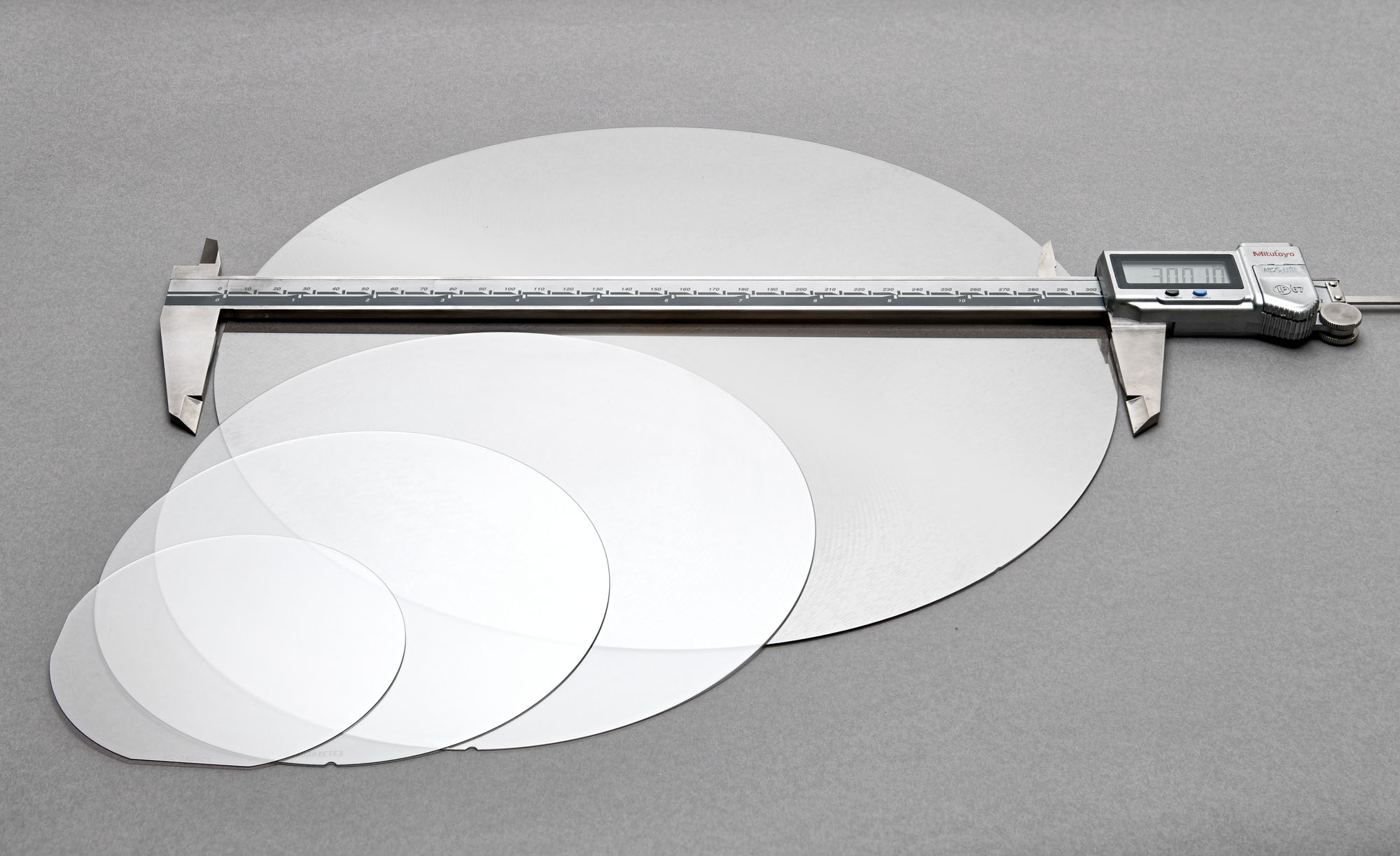
Wolfspeed 300mm silicon carbide wafer technology reached a historic milestone as the company successfully produced the world’s first 300mm (12-inch) single-crystal SiC wafer. This breakthrough strengthens Wolfspeed’s leadership in wide-bandgap semiconductors and creates a powerful foundation for next-generation electrification, data centers, and advanced power electronics across global markets.
Backed by an extensive intellectual property portfolio of more than 2,300 patents, this innovation pushes manufacturing scalability and performance to a new level. The larger wafer format significantly improves production economics while meeting the fast-rising demand from energy, mobility, and digital infrastructure sectors.
Why the Wolfspeed 300mm Silicon Carbide Wafer Matters
The transition to Wolfspeed 300mm silicon carbide wafer technology delivers clear technical and commercial advantages for high-power and high-efficiency applications.
Key benefits include:
These improvements are critical for industries that rely on fast, efficient, and reliable power conversion.
Driving Next-Generation Electrification and Digital Infrastructure
The Wolfspeed 300mm silicon carbide wafer unlocks substantial performance gains for fast-growing sectors such as electrification, AI data centers, and immersive computing. Larger SiC wafers enable more powerful and compact devices that can handle higher voltages and temperatures with minimal energy loss.
This directly supports:
By enabling higher power density and superior heat management, Wolfspeed’s 300mm platform accelerates the shift toward more efficient and sustainable electronic systems.
Unified Platform for Power, Optical, and RF Technologies
Beyond power electronics, the Wolfspeed 300mm silicon carbide wafer also integrates high-purity semi-insulating substrates designed for optical and RF applications. This creates a single wafer-scale platform that supports multiple domains, including power, thermal, optical, and photonic technologies.
This unified approach allows manufacturers to develop advanced systems with tighter integration, improved performance, and reduced complexity across industries ranging from communications to industrial automation.
By setting a new manufacturing standard, Wolfspeed is positioning silicon carbide at the center of the future electronics ecosystem, enabling faster innovation, lower system costs, and more energy-efficient technologies at scale.
Backed by an extensive intellectual property portfolio of more than 2,300 patents, this innovation pushes manufacturing scalability and performance to a new level. The larger wafer format significantly improves production economics while meeting the fast-rising demand from energy, mobility, and digital infrastructure sectors.
Why the Wolfspeed 300mm Silicon Carbide Wafer Matters
The transition to Wolfspeed 300mm silicon carbide wafer technology delivers clear technical and commercial advantages for high-power and high-efficiency applications.
Key benefits include:
- Higher device density per wafer, lowering cost per chip
- Improved thermal performance for high-power electronics
- Better energy efficiency in demanding operating conditions
- Greater manufacturing scalability for mass production
These improvements are critical for industries that rely on fast, efficient, and reliable power conversion.
Driving Next-Generation Electrification and Digital Infrastructure
The Wolfspeed 300mm silicon carbide wafer unlocks substantial performance gains for fast-growing sectors such as electrification, AI data centers, and immersive computing. Larger SiC wafers enable more powerful and compact devices that can handle higher voltages and temperatures with minimal energy loss.
This directly supports:
- Electric vehicle powertrains and fast-charging systems
- Grid and renewable energy infrastructure
- High-performance AI and cloud data centers
- AR and VR platforms requiring efficient power and thermal control
By enabling higher power density and superior heat management, Wolfspeed’s 300mm platform accelerates the shift toward more efficient and sustainable electronic systems.
Unified Platform for Power, Optical, and RF Technologies
Beyond power electronics, the Wolfspeed 300mm silicon carbide wafer also integrates high-purity semi-insulating substrates designed for optical and RF applications. This creates a single wafer-scale platform that supports multiple domains, including power, thermal, optical, and photonic technologies.
This unified approach allows manufacturers to develop advanced systems with tighter integration, improved performance, and reduced complexity across industries ranging from communications to industrial automation.
By setting a new manufacturing standard, Wolfspeed is positioning silicon carbide at the center of the future electronics ecosystem, enabling faster innovation, lower system costs, and more energy-efficient technologies at scale.
Company Press Release
Click above to visit the official source.
Share:
